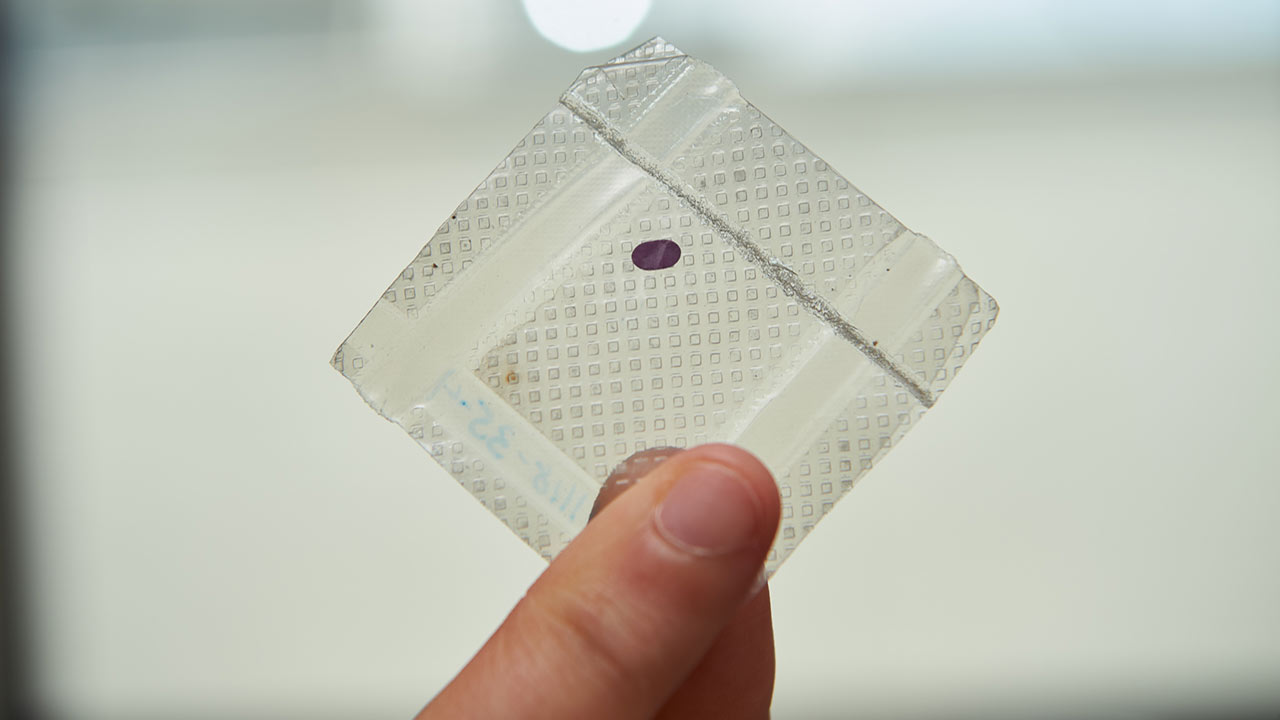
Thin-layer deposition is the process of creating and depositing thin film coatings onto a substrate material. These coatings can be made of many different materials, from metals to oxides to compounds. Different coatings have different characteristics which are leveraged to alter or improve aspects of the substrate performance. For example, some are transparent, some are very durable and scratch-resistant, and some increase or decrease the conductivity of electricity or transmission of signals.
Thin-layer deposition:
- Artificial retinas
- Semiconductors
- Sensors
The thin layers can be as small as a few atoms thick. Deposition can occur one layer at a time and has been referred to as “atomic-precision production.” Layers can influence each other, and layers are organized based on previous layers. The ability to “design-in” properties has led to breakthroughs in optical-, electrical-, and health-related industries. Common applications for thin-layer deposition solutions include dual-sided laser facet coating, wafer production, diamond-like carbon coatings, metallization, medical coatings, and lenses.
In microgravity, the absence of sedimentation and buoyancy allow dominant surface tension effects to result in more uniform and atomically and molecularly precise layering. The utilization of microgravity in the production of uniform thin layers has so far been limited, but the many potential opportunities make this an attractive target for a variety of industries.
Why conduct this research in space?
Thin-layer deposition in microgravity has applications in layering for medical devices and ceramic coatings.
For example:
- Microgravity enables precise layering for artificial retinas and other devices.
Examples of In-Space Production Applications Thin-Layer Deposition Projects
- Artificial Retinas
Microgravity enables greater uniformity and better film deposition, which can be used to produce precisely aligned, precisely structured layers of bacterial rhodopsin crystals (a light-activated protein to stimulate the retina of patients with impaired vision due to age-related macular degeneration and retinitis pigmentosa) sandwiched between layers of precisely deposited composite material with sufficient quality to enable an implantable artificial retina.
- Semiconductors
Semiconductors have countless uses in modern society. Thin-layer deposition in microgravity provides opportunities to produce enhanced systems, for example, in the production of chemical and radiation detection semiconductors. Such enhanced systems could potentially be more sensitive, more portable, and easier to scale.
In particular, graphene quality and properties produced in microgravity will be compared with graphene produced on Earth to better understand the effects gravity-induced convection has on nanomaterial production.
Results may lead to improved synthesis of nanomaterials in space and on Earth, enabling higher-performing sensors for the next generation of small, low-power radiation detectors and chemical analysis equipment.
- Sensors
Sensors based on semiconductors/microprocessors are critical components in detectors and analytical instruments like mass spectrometers, ion mobility spectroscopy, and radiation detectors. Improvements made through thin-layer deposition in microgravity can lead to improved sensitivity and enhanced capabilities.


